The Shift Register
The Shift Register: Complete Guide to Data Movement and Storage
Introduction to Shift Registers
In the realm of digital electronics, shift registers are among the most versatile and essential sequential logic circuits. While a single flip flop can store one bit of data, a shift register is a cascade of multiple flip flops connected together to store and move multiple bits of data simultaneously.
The defining characteristic of a shift register is its ability to shift data from one flip flop to the next on each clock pulse. This simple yet powerful operation enables shift registers to perform critical functions such as:
- Converting data between serial and parallel formats
- Temporarily storing data in digital systems
- Creating time delays
- Generating specific binary sequences
- Implementing arithmetic operations (multiplication/division by 2)
Shift registers are ubiquitous in modern electronics. They are found in microcontrollers for GPIO expansion, in communication interfaces like SPI and I2C, in LED displays, and in countless other applications where data needs to be moved, stored, or transformed.
This comprehensive guide will explore the different types of shift registers, their internal architecture, operational modes, and real-world applications, complete with visual diagrams and practical examples.
What is a Shift Register?
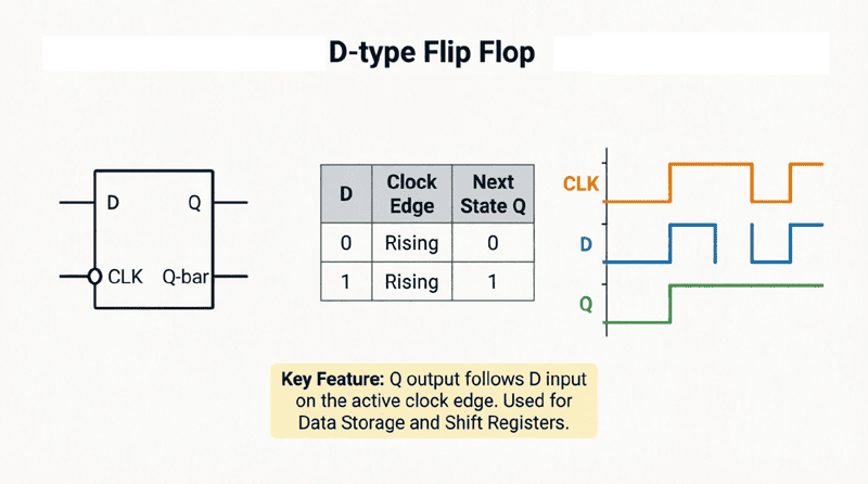
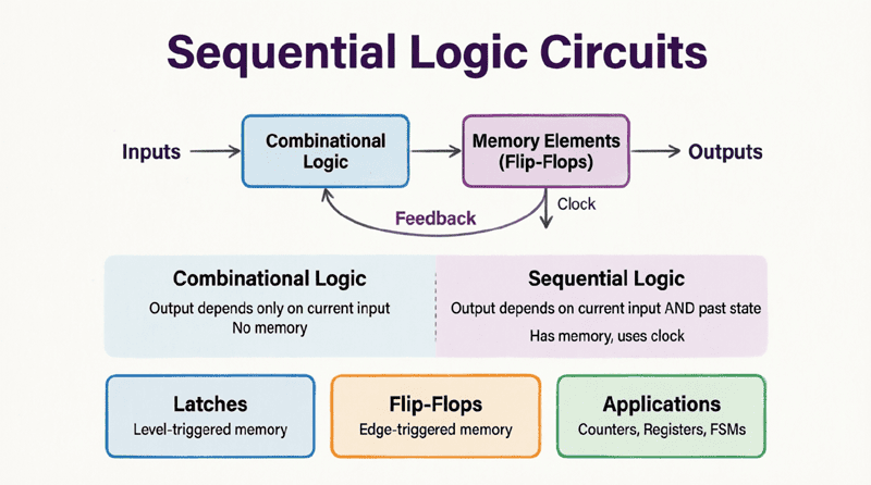
A shift register is a sequential logic circuit consisting of a cascade of flip flops (usually D-type) that share a common clock. It can store multiple bits of data and shift them from one flip flop to the next on each clock pulse. Shift registers are primarily used for serial-to-parallel or parallel-to-serial data conversion, temporary data storage, and creating time delays.
Basic Architecture and Operation
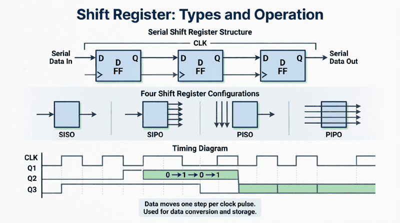
At its core, a shift register is simply a chain of D flip flops connected in series. The output (Q) of one flip flop is connected to the input (D) of the next flip flop. All flip flops share the same clock signal, ensuring synchronized operation.
How Data Shifts
Imagine a 4-bit shift register with four D flip flops labeled FF0, FF1, FF2, and FF3:
- Initial State: All outputs are 0 (Q0=0, Q1=0, Q2=0, Q3=0)
- Clock Pulse 1: A logic ‘1’ is applied to the input of FF0. On the clock edge, FF0 captures the ‘1’. Now: Q0=1, Q1=0, Q2=0, Q3=0
- Clock Pulse 2: A logic ‘0’ is applied to FF0’s input. On the clock edge:
- FF0 captures the ‘0’
- FF1 captures the previous value of Q0 (which was ‘1’)
- Result: Q0=0, Q1=1, Q2=0, Q3=0
- Clock Pulse 3: Another ‘0’ is applied. The ‘1’ shifts further right:
- Result: Q0=0, Q1=0, Q2=1, Q3=0
The data bit (‘1’) has literally shifted from left to right through the register, one position per clock pulse. This is the fundamental operation of all shift registers.
Direction of Shift
- Shift Right: Data moves from left (MSB) to right (LSB). This is the most common configuration.
- Shift Left: Data moves from right (LSB) to left (MSB).
- Bidirectional: Advanced shift registers can shift in either direction based on a control signal.
How does data shift in a shift register?
In a shift register, the Q output of each flip flop is connected to the D input of the next flip flop. On each clock pulse, every flip flop captures the value from its left neighbor (for right-shifting). This causes the data bits to move one position down the chain with each clock cycle, like people passing buckets in a fire brigade.
Types of Shift Registers
Shift registers are classified based on how data is entered (input) and retrieved (output). There are four primary configurations:
1. SISO (Serial-In, Serial-Out)
In a SISO shift register:
- Input: Data enters one bit at a time through a single serial input line.
- Output: Data exits one bit at a time through a single serial output line.
Operation:
- Data is shifted in serially, bit by bit.
- The data propagates through the chain of flip flops.
- After N clock pulses (where N is the number of bits), the first bit appears at the output.
- The register acts as a time delay or temporary storage buffer.
Applications:
- Time delay circuits
- Data buffering
- Serial data transmission
2. SIPO (Serial-In, Parallel-Out)
In a SIPO shift register:
- Input: Data enters one bit at a time through a single serial input line.
- Output: All bits are available simultaneously on separate parallel output lines (Q0, Q1, Q2, Q3…).
Operation:
- Serial data is shifted into the register bit by bit.
- Once all bits are loaded, they are all available at once on the parallel outputs.
- This is a serial-to-parallel converter.
Applications:
- Converting serial data from communication lines (UART, SPI) into parallel data for microprocessors
- Expanding GPIO pins on microcontrollers
- LED display drivers (e.g., 74HC595)
3. PISO (Parallel-In, Serial-Out)
In a PISO shift register:
- Input: All bits are loaded simultaneously through parallel input lines.
- Output: Data exits one bit at a time through a single serial output line.
Operation:
- Parallel data is loaded into all flip flops simultaneously (usually via a “Load” control signal).
- On subsequent clock pulses, the data is shifted out serially, one bit per clock.
- This is a parallel-to-serial converter.
Applications:
- Converting parallel data from microprocessors into serial data for transmission
- Reading multiple switches or sensors using a single input pin
- Data acquisition systems (e.g., 74HC165)
4. PIPO (Parallel-In, Parallel-Out)
In a PIPO shift register:
- Input: All bits are loaded simultaneously through parallel input lines.
- Output: All bits are available simultaneously on parallel output lines.
Operation:
- Data is loaded in parallel on one clock edge.
- Data appears at the outputs immediately (or on the next clock edge).
- No shifting occurs; this acts primarily as a temporary storage register or buffer.
Applications:
- Temporary data storage
- Data buffering between systems with different speeds
- Simple latches
What are the four types of shift registers?
- SISO (Serial-In, Serial-Out): Data enters and exits one bit at a time. Used for time delays.
- SIPO (Serial-In, Parallel-Out): Serial input, parallel output. Converts serial to parallel data.
- PISO (Parallel-In, Serial-Out): Parallel input, serial output. Converts parallel to serial data.
- PIPO (Parallel-In, Parallel-Out): Parallel input and output. Used for temporary storage.
The Universal Shift Register
While the four types above are distinct configurations, modern integrated circuits often combine these capabilities into a single device called a Universal Shift Register.
A universal shift register can:
- Shift data left
- Shift data right
- Load data in parallel
- Output data in parallel
- Output data serially
This versatility is achieved through multiplexers (MUX) at the input of each flip flop. Control signals (usually labeled S0, S1 or similar) select which data source is connected to each flip flop’s D input:
- Mode 00: Hold (no change)
- Mode 01: Shift Right
- Mode 10: Shift Left
- Mode 11: Parallel Load
Popular IC: The 74HC194 is a classic 4-bit universal shift register that demonstrates all these capabilities.
Practical Applications of Shift Registers
Shift registers are indispensable in modern digital systems. Here are their most common applications:
1. Serial-to-Parallel and Parallel-to-Serial Conversion
This is the primary function of shift registers in communication systems.
Example: UART Communication
When a computer sends data over a serial port (like RS-232 or USB), it uses a PISO shift register to convert parallel bytes from the CPU into a serial stream of bits. On the receiving end, a SIPO shift register converts the serial stream back into parallel bytes for the receiving CPU.
2. GPIO Expansion
Microcontrollers often have a limited number of General Purpose Input/Output (GPIO) pins. Shift registers allow you to expand these pins cheaply and easily.
Example: Driving 8 LEDs with 3 Pins
Using a SIPO shift register (like the 74HC595):
- Connect the microcontroller’s 3 pins to the shift register’s Data, Clock, and Latch pins.
- Send 8 bits of data serially (one bit per LED).
- The shift register converts this to 8 parallel outputs, each controlling one LED.
- You’ve just controlled 8 outputs using only 3 microcontroller pins!
3. LED Display Drivers
Shift registers are the backbone of LED matrix displays and 7-segment displays.
Example: 8-Digit 7-Segment Display
Instead of using 56 individual GPIO pins (8 digits × 7 segments), you can use shift registers to multiplex the display:
- Use a SIPO shift register to control which digit is active.
- Use another shift register to control which segments are lit.
- Rapidly scan through the digits (multiplexing) to create the illusion that all digits are lit simultaneously.
4. Data Storage and Delay Lines
SISO shift registers act as delay lines. If you need to delay a signal by N clock cycles, simply pass it through an N-stage shift register.
Applications:
- Digital signal processing (DSP)
- Timing alignment in high-speed circuits
- Creating specific time delays in control systems
5. Arithmetic Operations
Shifting data left or right performs simple arithmetic:
- Shift Left by 1: Multiplies the binary number by 2
- Shift Right by 1: Divides the binary number by 2
This is how early computers performed fast multiplication and division before dedicated arithmetic logic units (ALUs) became common.
6. Sequence Generators and Counters
By feeding the output of a shift register back to its input through logic gates, you can create:
- Ring Counters: The output of the last flip flop feeds back to the first.
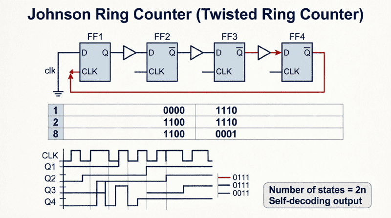
- Johnson Counters: The inverted output of the last flip flop feeds back to the first.
These are used in timing circuits, stepper motor control, and sequence generation.
Popular Shift Register ICs
Several integrated circuits have become industry standards for shift register applications:
74HC595 (SIPO – Serial-In, Parallel-Out)
- 8-bit shift register with output latches
- Cascadable: Connect multiple chips for more outputs
- Applications: LED drivers, GPIO expansion, output port expansion
- Features: Output enable pin, storage register latch
74HC165 (PISO – Parallel-In, Serial-Out)
- 8-bit parallel-load shift register
- Applications: Reading multiple switches, input port expansion
- Features: Parallel load capability, serial output
74HC164 (SIPO – Serial-In, Parallel-Out)
- 8-bit serial-in, parallel-out shift register
- Simpler than the 74HC595 (no output latch)
- Applications: Simple LED driving, basic serial-to-parallel conversion
74HC194 (Universal Shift Register)
- 4-bit bidirectional universal shift register
- Can shift left, shift right, or load in parallel
- Applications: Versatile data manipulation, educational purposes
Timing and Cascading
Cascading Shift Registers
One of the most powerful features of shift registers is their ability to be cascaded (connected in series) to create wider registers.
How to Cascade:
- Connect the Serial Output (Q7 or QH’) of the first register to the Serial Input (DS or SER) of the second register.
- Connect all Clock pins together.
- Connect all Latch pins together (if applicable).
- The microcontroller sends data as if it were a single, wider register.
Example: Cascading two 74HC595 chips creates a 16-bit output register. Cascading four creates a 32-bit register, and so on.
Timing Considerations
When working with shift registers, timing is critical:
Setup Time: Data must be stable before the clock edge.
Hold Time: Data must remain stable after the clock edge.
Clock Frequency: Shift registers have maximum clock speeds (typically 20-100 MHz for modern HC/HCT series).
Propagation Delay: There is a small delay between the clock edge and the output changing.
Shift registers are fundamental building blocks in digital electronics, bridging the gap between serial and parallel data domains. Their ability to store, shift, and convert data makes them indispensable in applications ranging from simple LED control to complex communication systems.
Key takeaways from this guide include:
- Four Primary Types:
- SISO: Serial-In, Serial-Out (time delays)
- SIPO: Serial-In, Parallel-Out (serial-to-parallel conversion)
- PISO: Parallel-In, Serial-Out (parallel-to-serial conversion)
- PIPO: Parallel-In, Parallel-Out (temporary storage)
- Universal Shift Registers: Combine all capabilities with control signals for shifting left, shifting right, and parallel loading.
- Core Applications:
- GPIO expansion (controlling many outputs with few pins)
- Serial communication (UART, SPI, I2C)
- LED display driving
- Data storage and delay lines
- Arithmetic operations (multiplication/division by 2)
- Popular ICs: The 74HC595 (SIPO), 74HC165 (PISO), and 74HC194 (Universal) are industry standards.
- Cascading: Multiple shift registers can be chained together to create arbitrarily wide data paths.
Whether you’re expanding the GPIO capabilities of an Arduino, designing a communication interface, or building a digital display system, shift registers provide an elegant, cost-effective solution for managing data flow in digital systems.