The D-type Flip Flop
The D-type Flip Flop: Complete Guide to Data Storage and Timing
Introduction to the D-type Flip Flop
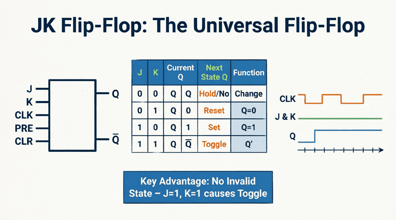
If the JK flip flop is the “universal” flip flop, the D-type (Data or Delay) flip flop is the undisputed workhorse of modern digital electronics. It is the most widely used memory element in digital systems, forming the foundational building block for registers, memory units, microprocessors, and complex data pipelines.
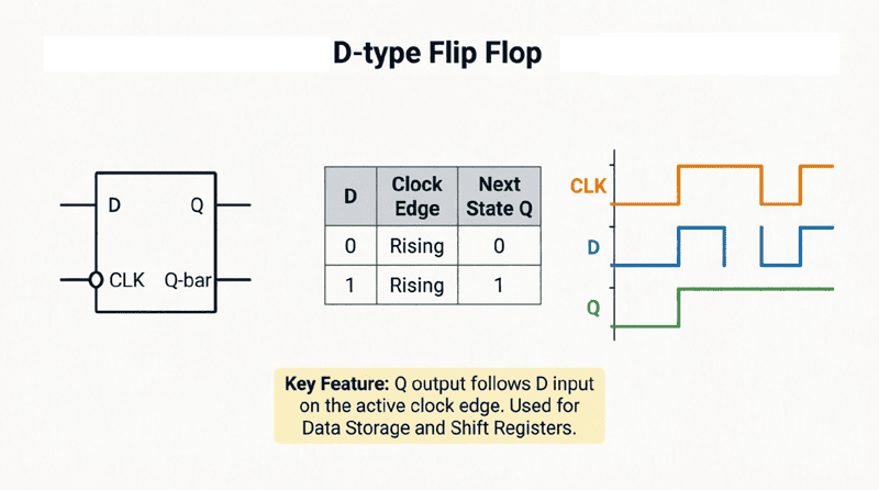
Unlike the SR or JK flip flops, which have two control inputs that dictate how the state should change, the D flip flop has a single data input. Whatever logic level is present at the D (Data) input is captured and transferred to the output Q on the active edge of the clock signal.
This elegant simplicity makes the D flip flop the ideal component for storing binary data, synchronizing asynchronous signals, and shifting data through digital circuits. Whether you are designing a simple 8-bit register or a multi-core CPU, the D flip flop is the fundamental cell that makes it all possible.
This comprehensive guide will explore the architecture, timing characteristics, truth table, and real-world applications of the D-type flip flop, complete with visual diagrams and technical explanations.
What is a D-type Flip Flop?
A D-type (Data or Delay) flip flop is a synchronous, edge-triggered memory element with a single data input (D). On the active edge of the clock signal, the logic level present at the D input is captured and transferred to the output (Q). It effectively “delays” the input data by one clock cycle, making it the standard building block for digital data storage and shift registers.
The Evolution: Why We Needed the D Flip Flop
To appreciate the D flip flop, we must look at the limitations of its predecessors.
The basic SR (Set-Reset) flip flop has a fatal flaw: the “forbidden state” where both S and R are HIGH, causing unpredictable outputs. The JK flip flop solves this by toggling the output when both J and K are HIGH.
However, in complex digital systems like computers, we often don’t want the circuit to toggle or hold; we simply want to store a specific bit of data (a 0 or a 1) at a precise moment. Using an SR or JK flip flop for this requires complex external logic to ensure the inputs are never in the forbidden or toggle states.
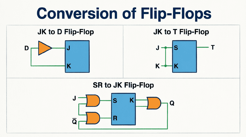
The D flip flop solves this elegantly. By adding a simple inverter (NOT gate) to an SR flip flop, we ensure that the Set and Reset inputs are always complementary. This completely eliminates the forbidden state and reduces the control interface to a single, intuitive “Data” line.
Internal Structure and Circuit Diagram
The most straightforward way to understand the D flip flop is to look at its internal logic gate diagram. It is typically constructed using an SR latch (made of NAND or NOR gates) preceded by an inverter.
The Inverter Mechanism
In a D flip flop, the single D input is connected directly to the Set (S) input of the underlying SR latch. The same D input is also fed through an inverter to the Reset (R) input.
Because of this inverter, S and R are always exact opposites:
- If D = 1, then S = 1 and R = 0 (Forces Q to 1).
- If D = 0, then S = 0 and R = 1 (Forces Q to 0).
This guarantees that S and R can never be 1 at the same time, completely eradicating the forbidden state.
Latch vs. Flip Flop
It is crucial to distinguish between a D Latch and a D Flip Flop:
- D Latch (Level-Triggered): The output follows the D input as long as the Enable/Clock pin is HIGH. It is “transparent” during the HIGH phase.
- D Flip Flop (Edge-Triggered): The output only updates at the exact moment the clock signal transitions (rising or falling edge). It ignores the D input at all other times. Modern digital design almost exclusively uses edge-triggered D flip flops.
What is the difference between a D Latch and a D Flip Flop?
A D Latch is level-triggered, meaning its output follows the D input as long as the clock/enable signal is HIGH. A D Flip Flop is edge-triggered, meaning it only captures the D input at the exact moment of the clock’s rising or falling edge, ignoring input changes at all other times.
Logic Symbol and Truth Table
The Logic Symbol
The standard logic symbol for a positive-edge-triggered D flip flop is a rectangle with:
- D on the left (Data input).
- CLK or > on the left, with a small triangle indicating edge-triggering.
- Q on the top right (Normal output).
- Q’ or $\overline{Q}$ on the bottom right (Inverted output).
- Optional PRE (Preset) and CLR (Clear) inputs at the top/bottom, usually marked with bubbles to indicate they are active-LOW.
The Truth Table
The operation of a positive-edge-triggered D flip flop is beautifully simple:
| Clock (CLK) | D (Data) | Q (Next State) | Operation |
|---|---|---|---|
| ↑ (Rising Edge) | 0 | 0 | Reset / Store 0 |
| ↑ (Rising Edge) | 1 | 1 | Set / Store 1 |
| 0 (Steady LOW) | X (Don’t Care) | Q (No Change) | Hold State |
| 1 (Steady HIGH) | X (Don’t Care) | Q (No Change) | Hold State |
| ↓ (Falling Edge) | X (Don’t Care) | Q (No Change) | Hold State |
(Note: “↑” represents the rising edge. “X” means the input state does not matter).
As the table shows, the flip flop only cares about the D input at the exact moment the clock rises. At all other times, the output Q remains locked in its previous state, regardless of what the D input is doing.
Timing Characteristics and Parameters
In high-speed digital design, simply knowing the truth table isn’t enough. The physical reality of electronic components introduces tiny delays. To ensure data is captured correctly, D flip flops have strict timing parameters that must be respected.
1. Setup Time ($t_{su}$)
Setup time is the minimum amount of time the D input must be stable and valid before the active clock edge arrives. If the D input changes too close to the clock edge, the flip flop might not capture the correct logic level.
2. Hold Time ($t_h$)
Hold time is the minimum amount of time the D input must remain stable after the active clock edge has passed. Even after the clock edge triggers the capture, the internal gates need a few nanoseconds to process the signal. If D changes immediately after the edge, it can corrupt the captured data.
3. Propagation Delay ($t_{pd}$)
Propagation delay is the time it takes for the output Q to actually change state after the active clock edge. It is never instantaneous. There are usually two specified delays:
- $t_{pLH}$: Time for Q to transition from LOW to HIGH.
- $t_{pHL}$: Time for Q to transition from HIGH to LOW.
4. Clock Pulse Width ($t_w$)
The clock pulse must remain HIGH (or LOW) for a minimum duration to ensure the internal master-slave latches have enough time to fully charge and transfer the data.
What are setup time and hold time in a D flip flop?
Setup time ($t_{su}$) is the minimum time the Data (D) input must be stable before the active clock edge. Hold time ($t_h$) is the minimum time the Data input must remain stable after the active clock edge. Violating these times can cause the flip flop to enter a metastable state or capture incorrect data.
Asynchronous Inputs: Preset and Clear
While the D and CLK inputs are synchronous (they only affect the output on the clock edge), most practical D flip flops include asynchronous inputs: Preset (PRE) and Clear (CLR) (sometimes labeled $\overline{S_D}$ and $\overline{R_D}$).
How They Work
These inputs override the clock and the D input entirely. They are typically active-LOW, meaning they are triggered when pulled to logic 0.
- Preset (PRE = 0, CLR = 1): Forces the output Q to 1 immediately, regardless of the clock or D input.
- Clear (PRE = 1, CLR = 0): Forces the output Q to 0 immediately.
- Normal Operation (PRE = 1, CLR = 1): Both asynchronous inputs are inactive, allowing the synchronous D and CLK inputs to control the flip flop.
- Invalid State (PRE = 0, CLR = 0): Both outputs are forced to 1, which is generally avoided in design.
These inputs are crucial for initializing a digital system. For example, when you turn on a computer, a “Power-On Reset” circuit pulls the CLR pin LOW on all flip flops to ensure the CPU starts with all registers cleared to zero.
Practical Applications of the D Flip Flop
The simplicity and reliability of the D flip flop make it the standard choice for a vast array of digital applications.
1. Data Storage and Registers
The primary use of the D flip flop is to store binary data. By grouping multiple D flip flops together and sharing a common clock, we create a Register.
- An 8-bit register consists of 8 D flip flops.
- On a single clock edge, 8 bits of parallel data are captured and stored simultaneously.
- This is the fundamental mechanism behind CPU registers, RAM memory cells, and buffer chips.
2. Shift Registers
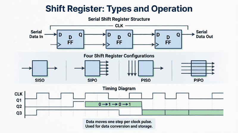
By connecting the Q output of one D flip flop to the D input of the next, and sharing the same clock, we create a Shift Register.
- Data is fed into the first flip flop’s D input.
- On each clock pulse, the data “shifts” one position to the right.
- This is heavily used in serial-to-parallel conversion (e.g., receiving data over a USB or SPI line and converting it to parallel bytes for a microprocessor).
3. Frequency Division (Toggle Mode)
Although the D flip flop doesn’t have a dedicated “toggle” input like the JK flip flop, it can easily be configured to divide frequency.
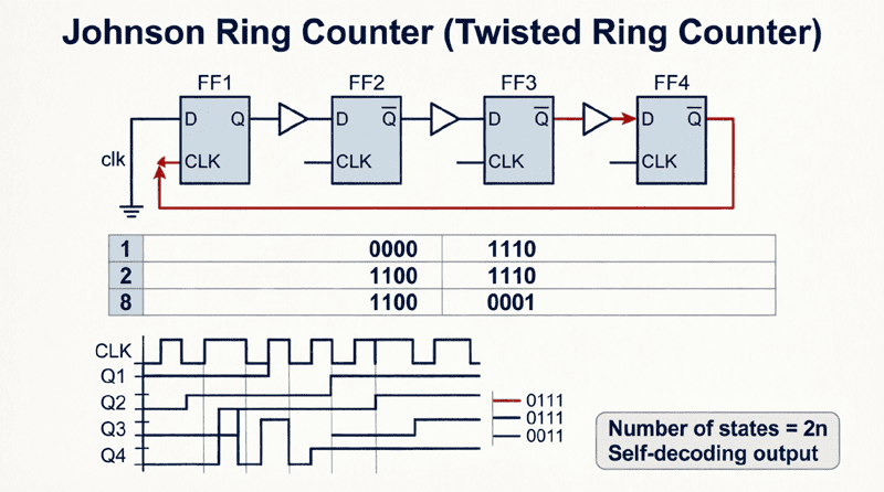
- Simply connect the inverted output (Q’) back to the D input.
- On the first clock edge, if Q is 0, Q’ is 1. This 1 is fed to D.
- On the next clock edge, the 1 is captured, making Q = 1 and Q’ = 0.
- The output toggles on every clock pulse, dividing the input frequency by exactly 2. Cascading these creates binary counters.
4. Input Synchronization (Debouncing)
In digital systems, external signals (like button presses or sensor inputs) are often asynchronous and “noisy” (bouncing). If fed directly into a complex state machine, this noise can cause catastrophic errors.
- A D flip flop is used to synchronize the signal.
- The noisy signal is fed into the D input, and a clean, stable system clock drives the CLK input.
- The output Q provides a clean, synchronized version of the input, aligned perfectly with the system clock.
The D-type flip flop is the cornerstone of synchronous digital design. By reducing the complex control inputs of the SR and JK flip flops into a single, intuitive Data line, it provides a robust, predictable, and simple method for storing and moving binary information.
Key takeaways from this guide include:
- Single Data Input: The D flip flop captures the logic level at the D input and transfers it to Q on the active clock edge.
- No Forbidden State: The internal inverter ensures the Set and Reset lines are always complementary, eliminating invalid states.
- Strict Timing Rules: Setup time ($t_{su}$) and hold time ($t_h$) are critical parameters that must be respected to prevent data corruption and metastability.
- Asynchronous Control: Preset and Clear pins allow the flip flop to be initialized or reset independently of the clock signal.
- Versatile Applications: From basic data registers and shift registers to frequency dividers and signal synchronizers, the D flip flop is ubiquitous in modern electronics.
Whether you are programming an FPGA, designing an ASIC, or building a discrete logic circuit on a breadboard, the D-type flip flop is the fundamental memory cell that will bring your digital designs to life.