I2C Voltage Level Translators
I2C Voltage Level Translators: Bi-Directional Level Shifting
Introduction to I2C Voltage Level Translation
In modern embedded systems and IoT devices, it’s common to encounter components operating at different voltage levels. Microcontrollers often run at 3.3V or even 1.8V for power efficiency, while sensors, displays, and legacy peripherals may require 5V logic levels. The I2C (Inter-Integrated Circuit) bus, one of the most popular communication protocols in embedded systems, frequently needs to bridge these different voltage domains.
I2C voltage level translators (also called level shifters) are essential circuits that enable safe and reliable communication between devices operating at different voltage levels. Unlike simple voltage dividers, I2C level translators must handle bi-directional data flow on both the SDA (data) and SCL (clock) lines while maintaining the open-drain characteristics of the I2C bus.
Understanding how to properly implement I2C level translation is crucial for:
- Interfacing 3.3V microcontrollers with 5V sensors and peripherals
- Connecting 1.8V mobile processors to 3.3V devices
- Protecting low-voltage ICs from overvoltage damage
- Ensuring reliable communication in mixed-voltage systems
- Maintaining signal integrity and bus timing
This comprehensive guide will explore the theory, circuits, and practical implementation of I2C voltage level translators, from simple MOSFET-based designs to dedicated IC solutions.
What is an I2C Voltage Level Translator?
An I2C voltage level translator is a bi-directional circuit that enables communication between I2C devices operating at different voltage levels (e.g., 3.3V and 5V). It safely translates logic levels on both SDA and SCL lines while maintaining the open-drain characteristics of the I2C bus, preventing damage to low-voltage components.
Understanding the I2C Bus Characteristics
Before diving into level translation techniques, it’s essential to understand the unique characteristics of the I2C bus that make level translation challenging.
Open-Drain Architecture
I2C uses open-drain (or open-collector) outputs, which means:
- Devices can only pull the line LOW (to ground)
- They cannot drive the line HIGH
- Pull-up resistors are required to bring the line HIGH
- Multiple devices can share the same bus without conflict
This open-drain configuration is fundamental to I2C operation and directly impacts how we design level translators.
Bi-Directional Data Flow
The I2C SDA (Serial Data) line is bi-directional:
- Masters can write data to slaves
- Slaves can acknowledge and send data back
- Both devices can pull the line LOW
- The direction can change within a single transaction
This bi-directional nature means level translators must work in both directions simultaneously, which eliminates simple unidirectional solutions like voltage dividers or level-shifting buffers.
Voltage Level Requirements
I2C devices have specific voltage thresholds:
- VIL (Input LOW): Maximum voltage recognized as logic 0 (typically 0.3 × VDD)
- VIH (Input HIGH): Minimum voltage recognized as logic 1 (typically 0.7 × VDD)
- VOL (Output LOW): Maximum voltage when driving LOW (typically < 0.4V)
- VOH (Output HIGH): For open-drain, this is the pull-up voltage
Example: For a 3.3V device:
- VIL max = 0.3 × 3.3V = 0.99V
- VIH min = 0.7 × 3.3V = 2.31V
For a 5V device:
- VIL max = 0.3 × 5V = 1.5V
- VIH min = 0.7 × 5V = 3.5V
This creates a challenge: a 3.3V HIGH (3.3V) may not be recognized as HIGH by a 5V device (needs 3.5V minimum), and a 5V signal can damage a 3.3V device.
Why can’t we use a simple voltage divider for I2C level shifting?
Voltage dividers are unidirectional and would prevent the bi-directional data flow required by I2C. Additionally, they would interfere with the open-drain architecture and could cause signal integrity issues. I2C requires bi-directional level translators that preserve the open-drain characteristics.
The MOSFET-Based Level Translator Circuit
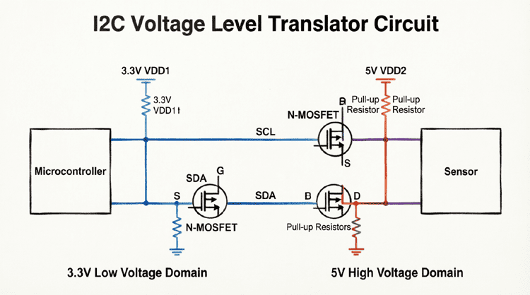
The most popular and elegant solution for I2C level translation is the MOSFET-based bi-directional level shifter, popularized by NXP (formerly Philips). This circuit uses a single N-channel MOSFET per I2C line (SDA and SCL) to achieve bi-directional level translation.
Circuit Configuration
Components Required (per line):
- 1 N-channel MOSFET (logic-level, low VGS(th))
- 1 Pull-up resistor to low voltage (e.g., 3.3V)
- 1 Pull-up resistor to high voltage (e.g., 5V)
Circuit Connections:
- LV (Low Voltage side): Connected to low-voltage I2C device (e.g., 3.3V MCU)
- HV (High Voltage side): Connected to high-voltage I2C device (e.g., 5V sensor)
- MOSFET Source: Connected to LV side
- MOSFET Drain: Connected to HV side
- MOSFET Gate: Connected to LV supply (e.g., 3.3V)
- Pull-up resistors: 2.2kΩ to 10kΩ on both LV and HV sides
How It Works
The circuit operates in three distinct states:
State 1: LV side drives LOW
- Low-voltage device pulls LV line to 0V
- MOSFET VGS = 3.3V – 0V = 3.3V (exceeds threshold)
- MOSFET turns ON, creating low-resistance path
- HV side is pulled LOW through MOSFET
- Result: Both sides LOW ✓
State 2: HV side drives LOW
- High-voltage device pulls HV line to 0V
- MOSFET body diode conducts initially
- LV side pulled to ~0.6V (diode drop)
- VGS = 3.3V – 0.6V = 2.7V (exceeds threshold)
- MOSFET turns ON, pulling LV fully LOW
- Result: Both sides LOW ✓
State 3: Both sides release (HIGH)
- Neither device drives the line
- MOSFET VGS = 3.3V – 3.3V = 0V (below threshold)
- MOSFET turns OFF
- LV pulled HIGH by LV pull-up (3.3V)
- HV pulled HIGH by HV pull-up (5V)
- Result: LV = 3.3V, HV = 5V ✓
MOSFET Selection Criteria
Choosing the right MOSFET is critical for reliable operation:
Key Parameters:
- VGS(th) – Gate Threshold Voltage:
- Must be low enough to turn on with VGS = VLV – Vdiode
- Typical requirement: VGS(th) < 1.5V
- Recommended: VGS(th) < 1.0V for margin
- VDS – Drain-Source Voltage:
- Must withstand the high voltage
- Requirement: VDS > HV supply
- Recommended: VDS ≥ 30V for 5V systems
- RDS(on) – On-Resistance:
- Lower is better for signal integrity
- Should be < 10Ω for I2C speeds
- Typical: 1-5Ω
- Gate-Source Voltage Rating:
- Must handle the low-voltage supply
- Requirement: VGS(max) > LV supply
Popular MOSFET Choices:
- BSH103: VGS(th) = 0.8V, VDS = 60V, RDS(on) = 2.5Ω
- 2N7000: VGS(th) = 1.0V, VDS = 60V, RDS(on) = 5Ω
- BSS138: VGS(th) = 0.8V, VDS = 50V, RDS(on) = 3.5Ω (most popular)
- ZXM61N02FTA: VGS(th) = 0.5V, VDS = 20V, RDS(on) = 0.25Ω
Practical Circuit Example
Design for 3.3V ↔ 5V Translation:
LV Side (3.3V)          HV Side (5V)
    |                       |
   4.7kΩ                   4.7kΩ
    |                       |
    +---- SDA_LV           +---- SDA_HV
    |                       |
    +---- SCL_LV           +---- SCL_HV
    |                       |
   ---                     ---
   GND                     GND

MOSFET (per line):
- Source → LV side
- Drain → HV side
- Gate → 3.3V supply
- Type: BSS138
Pull-up Resistor Selection:
- Standard I2C: 4.7kΩ to 10kΩ
- Fast-mode (400 kHz): 2.2kΩ to 4.7kΩ
- Fast-mode+ (1 MHz): 1kΩ to 2.2kΩ
- Consider bus capacitance and current limits
What MOSFET should I use for I2C level shifting?
The BSS138 is the most popular choice for I2C level translation. It has a low gate threshold (0.8V), adequate voltage rating (50V), and low on-resistance (3.5Ω). Other good options include BSH103, 2N7000, or ZXM61N02FTA for lower RDS(on).
Dedicated I2C Level Translator ICs
While discrete MOSFET solutions work well, dedicated I2C level translator ICs offer advantages in terms of integration, performance, and ease of use.
Popular I2C Level Translator ICs
1. Texas Instruments TXB0104/TXB0108
- 4-bit or 8-bit bi-directional translator
- Automatic direction sensing
- Voltage range: 0.95V to 3.6V (A port), 1.65V to 5.5V (B port)
- Maximum data rate: 20 Mbps
- Built-in pull-up resistors (optional)
- Advantages: No direction control needed, fast speeds
- Disadvantages: Not ideal for I2C (can have issues with long hold times)
2. NXP PCA9306
- Dual bi-directional I2C bus and SMBus translator
- Specifically designed for I2C
- Voltage range: 1.8V to 5.5V on both sides
- No enable pin required
- Supports clock stretching
- Advantages: I2C-optimized, simple design
- Disadvantages: Limited to 2 channels
3. Texas Instruments TCA39306
- Dual bi-directional I2C translator
- Ultra-low quiescent current
- Voltage range: 1.2V to 5.5V
- Enable pin for power management
- Supports hot-swap
- Advantages: Low power, robust design
- Disadvantages: Slightly higher cost
4. NXP PCA9515A
- I2C-bus repeater with level translation
- Voltage range: 2.3V to 5.5V
- Includes bus buffering
- Supports clock synchronization
- Advantages: Bus isolation, improved noise immunity
- Disadvantages: More complex, higher cost
When to Use Dedicated ICs vs. Discrete MOSFETs
Use Discrete MOSFETs When:
- Cost is critical (MOSFETs cost pennies)
- Simple 2-wire I2C interface
- Low to moderate speeds (< 400 kHz)
- Board space is available
- You need flexibility in voltage levels
Use Dedicated ICs When:
- Multiple I2C lines need translation
- High reliability is required
- Fast-mode+ or high-speed I2C (> 400 kHz)
- Board space is limited (smaller footprint)
- You need additional features (enable, fault protection)
- Production consistency is important
Practical Implementation Guidelines
PCB Layout Considerations
Proper PCB layout is essential for reliable I2C level translation:
1. Pull-up Resistor Placement:
- Place pull-ups close to the devices, not the level shifter
- Keep traces short to minimize capacitance
- Use ground plane for return paths
2. MOSFET Placement:
- Position MOSFETs close to connectors or voltage domain boundaries
- Minimize trace length between MOSFET pins
- Keep gate trace short and direct to LV supply
3. Decoupling:
- Add 0.1µF decoupling capacitors near voltage supplies
- Place capacitors close to IC power pins
- Use multiple vias for ground connections
4. Trace Routing:
- Keep SDA and SCL traces parallel and matched length
- Avoid routing near high-speed digital or analog signals
- Maintain adequate spacing (3× trace width minimum)
Common Design Mistakes
Mistake 1: Incorrect MOSFET Orientation
- Problem: Swapping source and drain connections
- Solution: Source always connects to LV side, drain to HV side
- Note: MOSFETs are symmetrical, but body diode direction matters
Mistake 2: Gate Connected to Wrong Voltage
- Problem: Connecting gate to HV instead of LV
- Solution: Gate must connect to the lower voltage supply
- Result: Wrong connection prevents MOSFET from turning on properly
Mistake 3: Missing Pull-up Resistors
- Problem: Relying on internal pull-ups only
- Solution: Always use external pull-ups on both sides
- Note: Some devices have weak internal pull-ups (20-50kΩ)
Mistake 4: Incorrect Pull-up Values
- Problem: Using values too high or too low
- Solution: Calculate based on bus capacitance and speed
- Formula: Rp(min) = (VCC – 0.4V) / 3mA (I2C spec)
Mistake 5: Exceeding MOSFET Ratings
- Problem: Using MOSFET with insufficient VDS or VGS ratings
- Solution: Always check datasheet ratings with margin
- Rule: VDS ≥ 2× HV voltage, VGS(th) < 1.5V
Testing and Debugging
Essential Tests:
- Voltage Level Verification:
- Measure LV side HIGH: Should equal LV supply
- Measure HV side HIGH: Should equal HV supply
- Measure LOW levels: Should be < 0.4V on both sides
- Bi-directional Communication:
- Test master-to-slave communication
- Test slave-to-master acknowledgment
- Verify clock stretching works (if applicable)
- Speed Testing:
- Start at standard mode (100 kHz)
- Test fast mode (400 kHz) if required
- Check for signal integrity with oscilloscope
- Stress Testing:
- Test with maximum bus capacitance
- Verify operation at voltage extremes
- Check temperature performance if needed
Debugging Tools:
- Oscilloscope: Essential for viewing waveforms and timing
- Logic Analyzer: Useful for decoding I2C transactions
- Multimeter: For checking DC voltage levels
- I2C Scanner: To verify device detection
Troubleshooting Common Issues
Issue 1: Communication fails in one direction
- Cause: MOSFET not turning on properly
- Check: VGS(th) specification, gate voltage
- Fix: Use MOSFET with lower VGS(th)
Issue 2: Slow rise times
- Cause: Pull-up resistors too large or bus capacitance too high
- Check: Rise time with oscilloscope (should be < 300ns for 400 kHz)
- Fix: Reduce pull-up resistance or add bus buffer
Issue 3: Intermittent communication
- Cause: Marginal signal levels or noise
- Check: Signal integrity, grounding, decoupling
- Fix: Improve layout, add decoupling capacitors
Issue 4: Device not detected
- Cause: Level shifter not passing signals
- Check: Continuity, MOSFET orientation, pull-ups
- Fix: Verify circuit connections and component values
Advanced Topics and Considerations
Multi-Voltage Systems
In complex systems with multiple voltage domains (1.8V, 3.3V, 5V), you may need:
- Cascaded level shifters for large voltage differences
- Separate level shifters for each voltage domain
- Careful planning of voltage translation hierarchy
I2C Bus Capacitance
The I2C specification limits total bus capacitance to 400pF. Level shifters add capacitance:
- MOSFET Ciss (input capacitance): ~20-50pF per device
- PCB trace capacitance: ~2-3pF per cm
- Device input capacitance: 5-10pF per device
Solutions:
- Use MOSFETs with low input capacitance
- Minimize trace lengths
- Add bus buffers for long buses
- Reduce pull-up resistance for faster rise times
Power Sequencing
When power supplies turn on/off in different sequences:
- Level shifters should not create back-powering paths
- Use MOSFETs with appropriate body diode characteristics
- Consider enable pins in dedicated ICs for controlled power-up
ESD Protection
I2C lines are susceptible to ESD damage:
- Add TVS diodes or ESD protection devices
- Choose MOSFETs with built-in ESD protection
- Follow proper PCB layout for ESD immunity
I2C voltage level translators are essential components in modern mixed-voltage embedded systems. Whether you choose a simple MOSFET-based circuit or a dedicated IC, understanding the principles of bi-directional level translation is crucial for reliable I2C communication.
Key takeaways from this guide:
- I2C Characteristics: Open-drain architecture and bi-directional data flow require special level translation techniques
- MOSFET Solution: The BSS138-based circuit is simple, cost-effective, and works reliably for most applications
- Dedicated ICs: Offer advantages for complex systems, high speeds, or production environments
- Proper Design: Correct MOSFET selection, pull-up resistor values, and PCB layout are critical for success
- Testing: Always verify bi-directional communication and signal integrity with proper test equipment
By following the guidelines in this article, you can confidently design robust I2C level translation circuits that enable seamless communication between devices operating at different voltage levels. Whether you’re interfacing a 3.3V Arduino with 5V sensors or connecting a 1.8V mobile processor to 3.3V peripherals, proper level translation ensures reliable, damage-free operation.