Passive Attenuator Tutorial
Passive Attenuator Tutorial: The Ultimate Design, Build, and Test Guide
Introduction to the Ultimate Passive Attenuator Tutorial
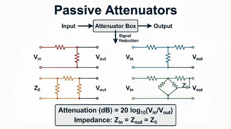
Welcome to the capstone of our comprehensive series on passive attenuators. In our other tutorials, we have dissected the L-pad, T-pad, Bridged-T, and Pi-pad networks. We have explored the mathematics of impedance matching, the nuances of bilateral symmetry, and the specific use cases for each topology.
But knowing the theory is only half the battle. The true challenge in RF and audio engineering lies in taking those mathematical formulas and turning them into a physical, reliable, and high-performance circuit. How do you choose the right topology when faced with a complex set of requirements? How do you select the physical resistors to ensure your 50Ω pad doesn’t turn into a reactive mess at 2 GHz? How do you verify your design using modern test equipment?
This ultimate Passive Attenuator Tutorial serves as your master guide. It ties together everything we have learned, providing a step-by-step workflow for designing, building, and testing passive attenuators for real-world applications. Whether you are a student building your first RF circuit or a seasoned engineer designing a precision test fixture, this tutorial will ensure your attenuator performs exactly as intended.
What is the ultimate goal of designing a passive attenuator?
The ultimate goal is to reduce a signal’s amplitude by a precise amount (in dB) while maintaining a strict characteristic impedance (e.g., 50Ω) across the desired frequency band, ensuring minimal signal reflection (VSWR) and flat frequency response.
Step 1: Choosing the Right Topology (The Decision Matrix)
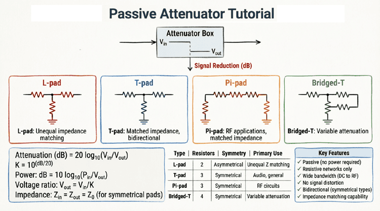
Before calculating a single resistor value, you must select the correct circuit topology. Choosing the wrong topology can lead to impractical resistor values, poor high-frequency performance, or an inability to meet your design goals. Use this decision matrix to guide your choice.
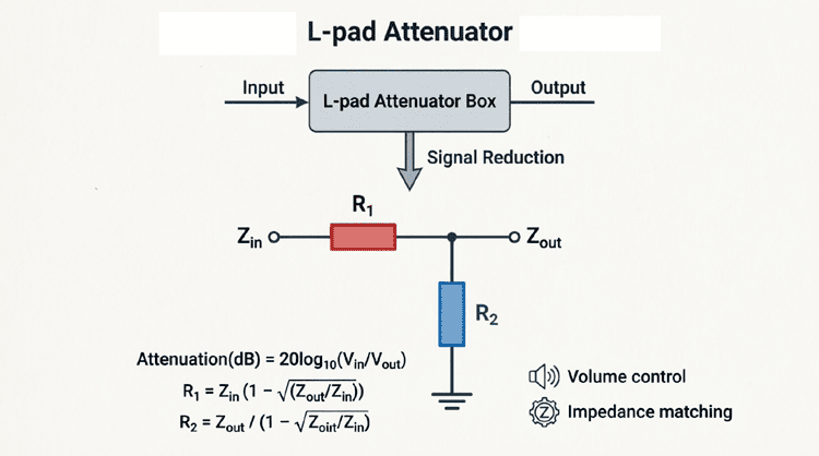
Scenario A: Unequal Impedance Matching ($Z_{in} \neq Z_{out}$)
If your source and load impedances are different (e.g., matching a 75Ω antenna to a 50Ω receiver), you must use an asymmetrical network.
- The Choice: L-pad Attenuator.
- Why: It is the only simple two-resistor network capable of matching unequal impedances.
- Caveat: It only matches impedance in one direction. If bidirectional matching is required, you must use a transformer or a more complex asymmetrical T or Pi network.
Scenario B: Equal Impedance, Fixed Attenuation ($Z_{in} = Z_{out}$)
If your system impedance is uniform (e.g., 50Ω) and you need a fixed amount of loss (e.g., a 10 dB pad).
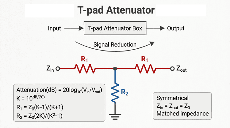
- Low Impedance Systems (≤ 75Ω): Choose the T-pad. It keeps the shunt resistor values relatively high, avoiding the parasitic inductance issues associated with very low-value resistors.
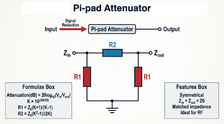
- High Impedance Systems (≥ 600Ω): Choose the Pi-pad. It keeps the shunt resistor values close to the system impedance, avoiding the impractical, tiny series resistors that a T-pad would require at high attenuation levels.
Scenario C: Equal Impedance, Variable Attenuation
If you need a continuously adjustable volume control or a stepped RF attenuator.
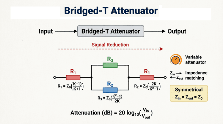
- The Choice: Bridged-T Attenuator.
- Why: The series resistors remain fixed at $Z_0$. Only the shunt and bridging resistors need to be varied. This allows for simple dual-gang potentiometers or 2-pole rotary switches, drastically simplifying the mechanical design compared to a T-pad or Pi-pad.
Which attenuator topology should I use for a 50Ω RF system?
For a fixed 50Ω RF attenuator, use a T-pad topology. It provides the most practical resistor values for low-impedance systems and minimizes the parasitic effects of low-value shunt resistors at high frequencies.
Step 2: The Universal Design Workflow
Once the topology is selected, follow this universal workflow to calculate and specify your components.
1. Define the Specifications
Clearly define your three core parameters:
- Characteristic Impedance ($Z_0$): Usually 50Ω, 75Ω, or 600Ω.
- Attenuation ($A_{dB}$): The desired signal loss in decibels.
- Power Handling ($P_{max}$): The maximum continuous RF power the attenuator must withstand without damage or drift.
2. Calculate the Attenuation Factor (K)
Convert the decibel value into a linear voltage ratio:
$$K = 10^{\frac{A_{dB}}{20}}$$
3. Calculate Resistor Values
Apply the specific formulas for your chosen topology (refer to the Quick Reference Cheat Sheet at the end of this article).
4. Select Standard Resistor Values
Calculated values rarely match standard E96 or E24 resistor series perfectly.
- Rule of Thumb: For RF attenuators, always round to the nearest 1% tolerance metal film resistor.
- Trimming: If you need ultra-precision (e.g., 0.1 dB accuracy), you must use resistor networks, trimmer potentiometers, or parallel/series combinations of standard resistors to hit the exact calculated value.
Step 3: Component Selection and Managing Parasitics
In DC circuits, a 50Ω resistor is always 50Ω. In RF circuits, a resistor is a complex network of resistance, parasitic series inductance ($L_s$), and parasitic parallel capacitance ($C_p$). At high frequencies, these parasitics ruin the attenuation flatness and destroy the impedance match.
Choosing the Right Resistor Type
- Carbon Composition: Excellent for RF up to a few hundred MHz. They have very low parasitic inductance but poor temperature stability and high tolerance.
- Thick Film (Standard SMD): Good for general use up to 1 GHz. However, the spiral laser trim used to set the resistance value introduces significant parasitic inductance.
- Thin Film (Precision SMD): The gold standard for RF attenuators. They have a straight resistive element (no spiral trim), resulting in ultra-low parasitic inductance. They are ideal for frequencies up to 10 GHz and beyond.
The “Low Value” Resistor Problem
When designing high-attenuation T-pads, the shunt resistor ($R_2$) becomes very small (e.g., 5Ω). At RF frequencies, the physical leads or pads of a 5Ω resistor will have an inductance of perhaps 1 nH. At 1 GHz, 1 nH has a reactance of $2\pi f L \approx 6.28 \Omega$. This means your 5Ω resistor is actually acting like a $5 + j6.28 \Omega$ impedance, completely ruining your 50Ω match!
- Solution: Use surface-mount (SMD) resistors (0402 or 0201 size) to minimize lead inductance, or use multiple higher-value resistors in parallel to achieve the low target resistance while averaging out the parasitics.
Step 4: PCB Layout and Construction
Building an attenuator on a breadboard is fine for audio, but disastrous for RF. At radio frequencies, the physical layout of the circuit is the circuit.
Microstrip and Ground Planes
For RF attenuators (especially 50Ω), the PCB must be designed as a controlled-impedance transmission line (usually microstrip or coplanar waveguide).
- Ground Plane: A solid, unbroken ground plane must exist directly beneath the signal trace.
- Ground Vias: Place multiple ground vias (stitched vias) immediately adjacent to the shunt resistors. This provides a low-inductance path to ground, which is critical for the shunt resistors to function correctly at high frequencies.
Component Placement
- Keep the signal path as short and straight as possible.
- Avoid right-angle bends in the PCB trace; use 45-degree chamfers or curved traces to prevent impedance discontinuities and signal reflections.
- Place the resistors as close together as physically possible to minimize the length of the transmission line between them.
How do I minimize parasitic inductance in an RF attenuator?
Use surface-mount (SMD) thin-film resistors in small packages (like 0402 or 0201). Avoid through-hole resistors, as their long leads introduce significant series inductance. Additionally, use a solid ground plane and place ground vias immediately next to the shunt resistors.
Step 5: Testing and Verification
Once your attenuator is built, you must verify that it meets your design specifications. Testing is done in two stages: DC verification and RF characterization.
Stage 1: DC Verification (The Multimeter Test)
Before applying RF power, use a high-quality digital multimeter to verify the resistor network.
- Measure the Resistors: Ensure $R_1$, $R_2$, and $R_3$ are within their specified tolerance.
- Measure Input Impedance: Connect the multimeter probes to the input port while the output port is terminated with a precision resistor equal to $Z_0$ (e.g., a 50Ω load). The multimeter should read exactly $Z_0$. If it doesn’t, check your solder joints and resistor values.
Stage 2: RF Characterization (The VNA Test)
To truly verify an RF attenuator, you must use a Vector Network Analyzer (VNA). The VNA measures the S-parameters of the network.
- S21 (Transmission / Insertion Loss): This measures the signal passing from port 1 to port 2. On a Log Magnitude plot, S21 should be a perfectly flat line at your target attenuation (e.g., -10 dB). If the line droops at high frequencies, your parasitic capacitance is too high. If it peaks, you have parasitic inductance causing resonance.
- S11 (Reflection / Return Loss): This measures how much signal is reflected back to the source. On a Smith Chart, the trace should be a tight dot exactly in the center (the 50Ω point). On a Log Magnitude plot, S11 should be as low as possible (e.g., < -20 dB). If S11 rises at high frequencies, your impedance match is degrading due to layout parasitics.
Power Testing
If the attenuator is designed for high power (e.g., 10W or 50W), you must perform a thermal test. Apply the maximum rated power and monitor the temperature of the resistors using a thermal camera. Ensure the resistors do not exceed their maximum operating temperature (usually 70°C to 125°C for SMDs). If they overheat, you must use larger physical resistors or add a heatsink to the PCB.
Quick Reference Formula Cheat Sheet
Here is a consolidated cheat sheet for designing symmetrical, equal-impedance attenuators.
First, calculate K:
$$K = 10^{\frac{A_{dB}}{20}}$$
T-Pad Formulas (Best for Low Z)
- Series Resistors: $R_1 = R_3 = Z_0 \left( \frac{K – 1}{K + 1} \right)$
- Shunt Resistor: $R_2 = Z_0 \left( \frac{2K}{K^2 – 1} \right)$
Pi-Pad Formulas (Best for High Z)
- Shunt Resistors: $R_1 = R_3 = Z_0 \left( \frac{K + 1}{K – 1} \right)$
- Series Resistor: $R_2 = Z_0 \left( \frac{K^2 – 1}{2K} \right)$
Bridged-T Formulas (Best for Variable)
- Series Resistors: $R_1 = R_3 = Z_0$ (Fixed)
- Shunt Resistor: $R_2 = \frac{Z_0}{K – 1}$
- Bridging Resistor: $R_4 = Z_0 \times (K – 1)$
Designing a passive attenuator is a perfect blend of elegant mathematics and rigorous physical engineering. The formulas for the L, T, Pi, and Bridged-T networks provide the theoretical foundation, but the real-world performance relies entirely on component selection, parasitic management, and precise PCB layout.
Key takeaways from this ultimate tutorial include:
- Topology Selection: Match the topology to the application. Use L-pads for unequal impedances, T-pads for low-impedance RF, Pi-pads for high-impedance audio/video, and Bridged-T for variable applications.
- Parasitics are the Enemy: At RF frequencies, a resistor is never just a resistor. Use SMD thin-film components and minimize lead lengths to prevent inductance and capacitance from ruining your impedance match.
- Layout is Critical: A solid ground plane, ground vias near shunt resistors, and controlled-impedance traces are mandatory for high-frequency performance.
- Verify with a VNA: DC resistance checks are not enough. You must measure S11 (return loss) and S21 (insertion loss) with a Vector Network Analyzer to ensure the attenuator performs correctly across your target frequency band.
By following this comprehensive workflow, you can confidently design, build, and test passive attenuators that perform flawlessly in any audio, RF, or test and measurement application. You now possess the complete toolkit required to master passive signal reduction.