The JK Flip Flop
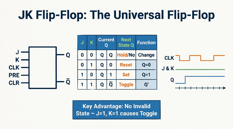
The JK Flip Flop: Complete Guide to Operation, Truth Table, and Toggle Mode
Introduction to the JK Flip Flop
In the world of sequential digital logic, the JK Flip Flop is often referred to as the “universal” flip flop. It is one of the most versatile and widely used memory elements in digital circuit design. Building upon the basic Set-Reset (SR) flip flop, the JK flip flop eliminates the “invalid” or “forbidden” state that plagues the SR design, replacing it with a highly useful “toggle” mode.
Because of its reliability, flexibility, and ability to divide frequencies, the JK flip flop is a fundamental building block in counters, shift registers, frequency dividers, and complex control logic. Understanding how it works is a critical milestone for any student or engineer studying digital electronics.
This comprehensive guide will explore the internal structure, logic operation, truth table, and advanced configurations of the JK flip flop, complete with visual diagrams and practical examples.
What is a JK Flip Flop?
A JK flip flop is a sequential logic circuit with two inputs (J and K), a clock input, and two complementary outputs (Q and Q’). It is an enhanced version of the SR flip flop that eliminates the invalid state. When both J and K are HIGH, the flip flop enters “toggle mode,” switching its output state on every clock pulse, making it ideal for counters and frequency division.
Evolution from the SR Flip Flop
To understand the brilliance of the JK flip flop, we must first look at its predecessor: the SR (Set-Reset) Flip Flop.
An SR flip flop has two inputs: Set (S) and Reset (R).
- If S=1 and R=0, the output Q is Set to 1.
- If S=0 and R=1, the output Q is Reset to 0.
- If S=0 and R=0, the output holds its previous state.
However, if S=1 and R=1, both outputs (Q and Q’) are forced to 0. This violates the rule that Q and Q’ must be complementary (opposites). When the inputs return to 0 simultaneously, the final state becomes unpredictable. This is known as the invalid or forbidden state.
The JK flip flop was invented to solve this problem. By adding feedback from the outputs (Q and Q’) back to the inputs, the JK flip flop ensures that when both inputs are HIGH, the circuit doesn’t enter an invalid state. Instead, it toggles its output.
Internal Structure and Circuit Diagram
The basic JK flip flop is typically constructed using NAND gates. It consists of two input NAND gates (with three inputs each) and two cross-coupled NAND gates that form the basic SR latch.
The Feedback Mechanism
The secret to the JK flip flop’s operation lies in its feedback loops:
- The J input is combined with the Q’ (complement) output in the first NAND gate.
- The K input is combined with the Q output in the second NAND gate.
This feedback ensures that only one of the input NAND gates can be activated at a time, preventing the invalid state. For example, if Q is currently 1 (and Q’ is 0), the J input is effectively “blocked” because the NAND gate requires all inputs to be 1 to output a 0. Only the K input can affect the circuit.
How does the JK flip flop avoid the invalid state of the SR flip flop?
The JK flip flop uses feedback from its outputs (Q and Q’) to its inputs. This feedback mechanism ensures that when both J and K are HIGH, the circuit is forced to toggle its state rather than entering the unpredictable, invalid state found in basic SR flip flops.
Truth Table and Logic Operation
The behavior of the JK flip flop is best understood through its truth table. The outputs change state on the active edge of the clock signal (either the rising or falling edge, depending on the specific design).
| Clock | J | K | Q (Next State) | Q’ (Next State) | Operation |
| :—: | :-: | :-: | :—: | :—: | :— |
| ↓ | 0 | 0 | Q (No Change) | Q’ (No Change) | Hold / Memory |
| ↓ | 0 | 1 | 0 | 1 | Reset |
| ↓ | 1 | 0 | 1 | 0 | Set |
| ↓ | 1 | 1 | Q’ (Toggle) | Q (Toggle) | Toggle |
(Note: “↓” represents the active clock edge, usually the falling edge in standard NAND-based designs).
Breakdown of the Four Modes
1. Hold Mode (J=0, K=0):
When both inputs are LOW, the flip flop ignores the clock pulse. The outputs remain exactly as they were. This is the “memory” state.
2. Reset Mode (J=0, K=1):
When J is LOW and K is HIGH, the flip flop is forced into the Reset state. The output Q becomes 0, and Q’ becomes 1 on the next clock edge.
3. Set Mode (J=1, K=0):
When J is HIGH and K is LOW, the flip flop is forced into the Set state. The output Q becomes 1, and Q’ becomes 0 on the next clock edge.
4. Toggle Mode (J=1, K=1):
This is the magic of the JK flip flop. When both inputs are HIGH, the output switches to its opposite state. If Q was 1, it becomes 0. If Q was 0, it becomes 1. This happens on every single clock pulse.
The Toggle Mode and Frequency Division
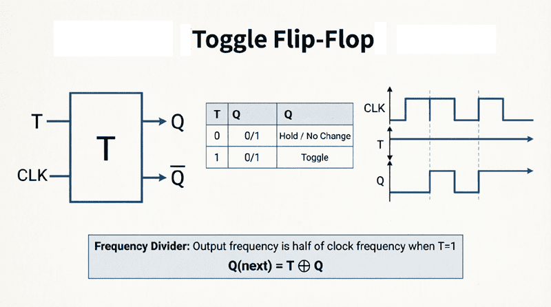
The Toggle mode is the most unique and powerful feature of the JK flip flop. When J and K are tied HIGH together, the flip flop acts as a T (Toggle) Flip Flop.
How Frequency Division Works
Imagine you feed a 100 Hz square wave clock signal into a JK flip flop configured in toggle mode (J=1, K=1).
- On the first clock pulse, Q goes HIGH.
- On the second clock pulse, Q goes LOW.
- On the third clock pulse, Q goes HIGH again.
It takes two clock pulses for the output Q to complete one full cycle (HIGH to LOW and back to HIGH). Therefore, the output frequency is exactly half of the input clock frequency.
Output Frequency = Input Clock Frequency / 2
This makes the JK flip flop an excellent frequency divider or binary counter. By cascading multiple JK flip flops (connecting the Q output of the first to the clock input of the second), you can divide the frequency by 4, 8, 16, and so on.
What is the toggle mode in a JK flip flop?
Toggle mode occurs when both J and K inputs are HIGH. In this state, the flip flop’s output (Q) switches to its opposite logic level on every active clock edge. This effectively divides the input clock frequency by two, making it essential for building binary counters and frequency dividers.
The Race-Around Condition and the Master-Slave JK Flip Flop
While the basic JK flip flop solves the invalid state problem, it introduces a new issue if it is level-triggered (where the output can change as long as the clock is HIGH).
The Race-Around Condition
If J=1 and K=1, and the clock pulse remains HIGH for a relatively long time, the output Q will toggle. However, this new Q is immediately fed back to the inputs. Because the clock is still HIGH, the flip flop will toggle again, and again, and again. The output will oscillate rapidly between 0 and 1 for the entire duration of the clock pulse. This chaotic behavior is called the race-around condition.
The Solution: Master-Slave Configuration
To eliminate the race-around condition, engineers developed the Master-Slave JK Flip Flop. This configuration uses two separate SR flip flops connected in series: the Master and the Slave.
- The Master: Receives the J and K inputs and is triggered by the rising edge (or HIGH level) of the clock. It captures the input data but its output is not sent to the final Q terminal.
- The Inverter: An inverter connects the clock of the Master to the clock of the Slave.
- The Slave: Receives the output from the Master and is triggered by the falling edge (or LOW level) of the clock. It updates the final Q and Q’ outputs.
How it fixes the problem: Because the Master and Slave are active on opposite halves of the clock cycle, the feedback loop is broken during the active phase. The Master captures the state, waits for the clock to fall, and then passes it to the Slave. This ensures the output toggles exactly once per clock cycle, completely eliminating the race-around condition.
Timing Diagrams and Waveforms
Understanding the timing diagram is crucial for visualizing how the JK flip flop responds to inputs over time.
Key Timing Characteristics
- Setup Time ($t_{su}$): The minimum time the J and K inputs must be stable before the active clock edge.
- Hold Time ($t_h$): The minimum time the J and K inputs must remain stable after the active clock edge.
- Propagation Delay ($t_p$): The time it takes for the output Q to change after the active clock edge.
In a timing diagram, you will see the Clock, J, K, and Q waveforms. Notice that Q only changes state precisely at the clock edge. If J and K change while the clock is steady, Q remains completely unaffected, highlighting the stability of edge-triggered (or master-slave) designs.
Practical Applications of the JK Flip Flop
The versatility of the JK flip flop makes it a staple in digital system design. Here are its most common applications:
1. Binary Counters
By connecting the Q output of one JK flip flop to the clock input of the next, and tying all J and K inputs HIGH, you create an asynchronous (ripple) counter. Each stage divides the frequency by 2, creating a binary counting sequence (00, 01, 10, 11).
2. Frequency Dividers
As mentioned in the toggle mode section, a single JK flip flop divides a clock signal by 2. Cascading them creates dividers by 4, 8, 16, etc., which is essential in microprocessor clock generation and digital communication.
3. Shift Registers
By connecting the Q output of one flip flop to the J input of the next (and Q’ to K), and applying a serial data stream to the first flip flop, you can create a shift register. This is used to convert serial data to parallel data (and vice versa) in communication protocols like SPI and UART.
4. Control Logic and Sequence Generators
JK flip flops are used in Finite State Machines (FSMs) to remember the current state of a system. They are heavily used in traffic light controllers, vending machines, and automated manufacturing sequences.
5. Johnson and Ring Counters
By feeding the inverted output (Q’) of the last flip flop back to the input of the first, JK flip flops can be configured into Johnson Ring Counters, which are used for generating specific timing sequences and controlling stepper motors.
The JK flip flop is a masterpiece of digital logic design. By elegantly solving the forbidden state limitation of the SR flip flop through output feedback, it introduced the highly useful toggle mode. This single feature makes it the undisputed king of counting and frequency division applications.
Key takeaways from this guide include:
- Universal Nature: The JK flip flop can mimic the behavior of SR, D, and T flip flops, making it the most versatile memory element.
- Truth Table Mastery: J=0/K=0 holds state; J=0/K=1 resets; J=1/K=0 sets; J=1/K=1 toggles.
- Toggle Mode: Tying J and K HIGH turns the flip flop into a frequency divider, outputting half the clock frequency.
- Race-Around Condition: Level-triggered JK flip flops can oscillate wildly if the clock pulse is too long.
- Master-Slave Solution: Using two latches triggered on opposite clock edges completely eliminates the race-around condition, ensuring reliable, single-toggle operation.
Whether you are designing a simple LED chaser, a complex microprocessor control unit, or a digital clock, the JK flip flop provides the reliable, predictable memory and counting capabilities required to bring your digital designs to life.